In previous experiments, the induction motor dq model and its controller was developed and tested in simulation and real-time. The power processing unit was considered a black-box that generated desired voltage at the inverter output given a reference voltage. In this experiment, the functioning of the power processing unit and the modulation algorithm used is explored in detail. Next section deals with the theoretical background for this experiment followed by simulation of switched-mode DC-AC converter. Finally, the simulation model is verified in real-time.
Consider the 3Φ 2 level inverter shown below:
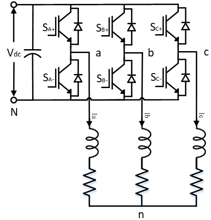
At no instant, can both switches of a leg be simultaneously ON, as this will lead to shoot-through because of directly shorting the DC bus. Thus, switches SA+ and SA- cannot be ON simultaneously. Similarly, switches SB+ and SB-, and SC+ and SC- cannot be ON simultaneously. If both switches in a leg are simultaneously turned OFF, the current through the load inductor free-wheels through the body-diode depending on the current direction. Thus, at any given instant, one-and-only one switch in a leg must be conducting. When switch SA+ is ON, the phase A output voltage with respect to DC bus neutral VaN = Vdc. When switch SA- is ON, VaN = 0. Similarly, the other phase output voltages can be controlled by turning ON and OFF their respective switches. The common-mode voltage, VnN, i.e. the voltage between the load's neutral terminal n and DC bus negative N is given by Eqn. 1 and the phase voltages Van, Vbn and Vcn are given by Eqns. 2, 3 and 4:
VnN = VaN + VbN +VcN3(1)
Van = VaN - VnN(2)
Vbn = VbN - VnN(3)
Vcn = VcN - VnN(4)
The output voltage of each of the phase can be controlled by adjusting the ratio of the top switch of a leg being turned ON to that of the bottom switch being turned ON. If SA+ is switched ON for time Ton and SA- is switched ON for time Toff alternatively, then the average output voltage is given by Eqn. 5. In pulse width modulation, the total, Ton + Toff is held constant, called the switching period, Tprd. Inverse of this gives the switching frequency. As Ton is varied from 0 to Tprd, the output voltage varies between 0 and Vdc. The duty-cycle is the ratio of switching period during which, switch SA+ must be held ON to generate the desired output voltage, as given in Eqn. 6. Similarly, the duty-cycles for phase B and C are obtained.
VaN = Ton,A+Ton,A+ + Toff,A+ × Vdc = dutyA × Vdc(5)
dutyA = VaNVdc(6)
The duty-cycles of the 3Φs can be modulated to generated desired output voltage at the inverter terminals. One such modulation algorithm that does this is the Sine-PWM (SPWM). In this method, the 3Φ duty-cycles are generated from the desired 3Φ sinusoidal reference output phase voltages as given by Eqns. 7,8 and 9.
dutyA = 12 + VanVdc(7)
dutyB = 12 + VbnVdc(8)
dutyC = 12 + VcnVdc(9)
If the desired 3Φ output voltages are balanced 3Φ sinusoidal voltages, as is the case here, above equations can be re-written as:
dutyA = 12 + m × sin(θ)(10)
dutyB = 12 + m × sin(θ -2π3)(11)
dutyC = 12 + m × sin(θ -4π3)(12)
where, m is the modulation index, which is the ratio of peak output phase voltage to that of the DC bus voltage:
m = Vph,peakVdc(13)
To generate the gate signal for switch SA+ from dutyA, the duty-cycle is compared with a triangular carrier that varies from 0 to 1. The triangular carrier repeats every 1/fswitch, where fswitch is the desired switching frequency. In SPWM, the reference output voltage was used for generating the duty-cycles. This limits the maximum magnitude of the modulation index to 0.5. As can be seen from Eqn. 10-12, if the modulation index were to exceed this limit, the output becomes saturated since the duty-cycles goes above the range [0, 1]. With this method, the peak line-line output voltage is limited to √32Vdc. This is not the maximum achievable output voltage and this limitation is overcome in the Space-vector pulse-width-modulation (SVPWM).
In SVPWM, the fact that the load's neutral point n is floating is used to further increase the range of the output voltage. It must be noted that if all the 3Φ duty-cycles were the same, the phase voltage of each of the phase i.e., Van, Vbn and Vcn are all 0, even though the output terminal to DC bust neutral i.e, VaN, VbN and VcN needn't be zero. This equal application of voltage on all 3Φs only leads to common mode voltage given in Eqn. 1 and not net potential difference between the output terminals. This is used to increase the output voltage range by modifying the duty-cycle equation as given below:
dutyA = 12 + m × (sin(θ) + sin(3θ)6)(14)
dutyB = 12 + m × (sin(θ -2π3) + sin(3θ)6)(15)
dutyC = 12 + m × (sin(θ -4π3) + sin(3θ)6)(16)
The addition of the third-harmonic component, sin(3θ)6, allows the modulation index to go as high as 1√3. Thus, the peak line-line output voltage can be up to Vdc using SVPWM compared to 12 using SPWM. It must be noted that regardless of addition of third-harmonic component, the output phase voltages are sinusoidal with only fundamental component (ignoring switching frequency components). The third-harmonic components only appear as common-mode voltage since they are the same in all 3Φs.
The same algorithm can be implemented in different ways using other combination of odd-triplen harmonics, all producing the same theoretical maximum output voltage. The duty-cycles for one such method avoids the direct computation of the third harmonic component is given below:
dutyA = 12 + m × (sin(θ) - dutyk2)(17)
dutyB = 12 + m × (sin(θ -2π3) - dutyk2)(18)
dutyC = 12 + m × (sin(θ -4π3) - dutyk2)(19)
dutyk = max(sin(θ), sin(θ -2π3), sin(θ -4π3)) + min(sin(θ), sin(θ -2π3), sin(θ -4π3))(20)
The above operation is simulated in this section using Workbench.
Sine-PWM:
Create a new project, and add a new model file to the project.
Set this model file as the Start model/Function in project properties.
Drag and drop the following tools from the Toolbox and connect them as shown.
| # | Tool type | Tool class | Tool name |
|---|---|---|---|
| 1 | Sine | Signal Sources | Sine |
| 2 | Gain | Math Block | Gain |
| 3 | Increment | Math Block | Increment |
| 4 | Triangle | Signal Sources | Triangle |
| 5 | Mag-Time Scope | Display | Scope |
| 6 | Comparator | Logical Block | Comparator |
| 7 | Boolean-Numeric cast | Signal Conversion | TypeCast |
| 8 | Gain | Math Block | Gain1 |
| 9 | Demux | Signal Routing | Demux |
| 10 | Adder Subtractor | Math Block | Add |
| 11 | Adder Subtractor | Math Block | Add1 |
| 12 | Gain | Math Block | Gain2 |
| 13 | Moving Average | Discrete | MovingAvg |
| 14 | Adder Subtractor | Math Block | Add2 |
| 15 | Mag-Time Scope | Display | Scope1 |
| 16 | Mag-Time Scope | Display | Scope2 |
| 17 | Demux | Signal Routing | Demux1 |
| 18 | Moving Average | Discrete | MovingAvg1 |
| 19 | Mag-Time Scope | Display | Scope3 |
| 20 | Mag-Time Scope | Display | Scope4 |
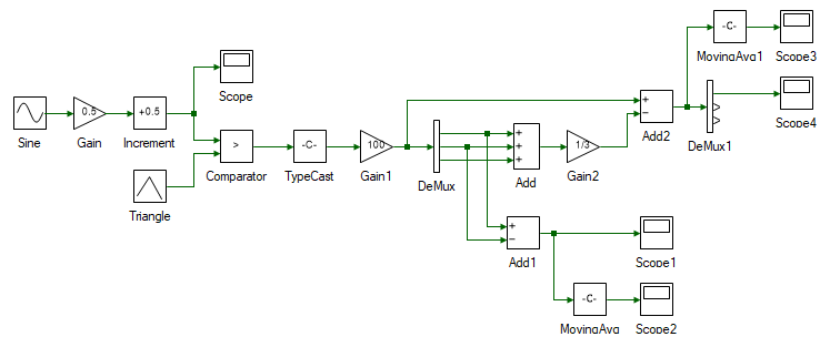
Change the properties of each tool to values listed in table below. Reason for each of those values are mentioned in the right-most column. To access a tool's property, double click on the tool and its properties will show up in the Properties dock.
| Tool name | Property field | Property value | Comments |
|---|---|---|---|
| Sine | Phase shift | {0, -120, -240} | 3Φ reference voltage signal. |
| Sine | Frequency | 50 | 50 Hz reference voltage. |
| Gain | Gain | 0.5 | Maximum modulation index in Eqns. 7 through 9. |
| Increment | Offset | 0.5 | 0.5 offset in Eqns. 7 through 9. |
| Triangle | Frequency | 10000 | Carrier/switching frequency is 10 kHz. |
| Triangle | Waveform | Triangle | Choosing triangular carrier over sawtooth, reduces the THD and switching losses compared to sawtooth, for this converter. |
| Scope | - | - | Scope to display the 3Φ duty-cycles. |
| Comparator | Function | < | Compares triangle carrier to dutyA, dutyB and dutyC, and if the former is greater, outputs True else False. |
| TypeCast | - | - | True/False does not have any intrinsic numeric value to it. This tool converts True to 1 and False to 0. Other values can be chosen as well in the properties. |
| Gain1 | Gain | 100 | When switch is ON, i.e. output of TypeCast is 1, the output voltage is 100 V. This scales the gate signal by the DC bus voltage to model an ideal switch. |
| Demux | Number of ports | 3 | Split the muxed 3Φ terminal voltages to individual components VaN, VbN and VcN. |
| Add | Number of ports | 3 | Computing the common-mode voltage in Eqn. 1. |
| Add1 | Arithmetic operation | +- | Line-line voltage Vab = VaN - VbN. |
| Gain2 | Gain | 1/3 | Computing the common-mode voltage in Eqn. 1. |
| MovingAvg | Number of Samples | 100 | Averaging the output line-line voltage Vab, between a switching period. |
| Add2 | Arithmetic operation | +- | Computing the 3Φ output phase voltages in Eqn. 2-4. |
| Scope1 | - | - | Scope to display Vab switching voltage. |
| Scope2 | - | - | Scope to display Vab average voltage. |
| MovingAvg1 | Number of Samples | 100 | Averaging the output phase voltage Van, between a switching period. |
| Demux1 | Number of ports | 3 | Split the muxed 3Φ phase voltages to individual components Van, Vbn and Vcn. |
| Scope3 | - | - | Scope to display Van average voltage. |
| Scope4 | - | - | Scope to display Van switching voltage. |
Since the carrier frequency is set to 10 kHz, the simulation is run at least 100 times faster than the carrier frequency to have results with sufficient resolution. Set the model step time to 1/(10 kHz)/100 = 1E-6 s. To do this, double click anywhere on the blank space in the model file. This opens up the model properties in the Properties dock. Change the Step time from 0.01 to 1E-6.
While at it, change the Run time from 10 to 0.05.
Run the simulation and observe the scope result. The phase voltage Van and line-line voltage Vab are shown in Scope4 and Scope1 respectively. Their waveform after filtering the switching-frequency component are shown in Scope3 and Scope4. Verify that the frequency, waveform and magnitude are as expected. So, far, the carrier waveform has been generated. In the next few steps this carrier will be compared with reference voltage to generate the switching signals.
Re-run the simulation for different output voltage. Change the output voltage by adjusting the gain of the Gain block from 0 to 0.5 and observe the results. Also make note of the generated output waveform when the gain is set to 1/√3.
Space vector PWM - Third harmonic injection:
Create a new project, and add a new model file to the project.
Set this model file as the Start model/Function in project properties.
Open the previously created Sine-PWM model file. Select all the tools in the model CtrlA and copy them CtrlC.
Paste CtrlV the copied model into the newly created model file.
Edit the pasted model by adding a third harmonic component to the reference Sine as shown below. The newly added tools are highlighted in green.
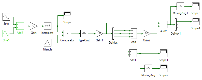
Set the property of the newly added Sine1 tool as given below.
| Tool name | Property field | Property value | Comments |
|---|---|---|---|
| Sine1 | Magnitude | 1/6 | 3rd harmonic voltage's magnitude as given by Eqns. 14 through 16. |
| Sine | Phase shift | 0 | 3rd harmonic voltages are in phase. |
| Sine | Frequency | 150 | 3rd harmonic voltages' frequency is three times the fundamental frequency. |
Set the model run time to 0.05s and step time to 1E-6 s.
Run the simulation and observe the scope result.
Re-run the simulation for different output voltage. Change the output voltage by adjusting the gain of the Gain block from 0 to 1/√3 and observe the results. Re-run the simulation for a gain value greater than 1/√3 and observe the results.
Space vector PWM - Min-max method:
Create a new project, and add a new model file to the project.
Set this model file as the Start model/Function in project properties.
Open the previously created Sine-PWM model file. Select all the tools in the model CtrlA and copy them CtrlC.
Paste CtrlV the copied model into the newly created model file.
Edit the pasted model by adding the tools highlighted in green to implement the min-max method as given by Eqns. 17 through 19.
| # | Tool type | Tool class | Tool name |
|---|---|---|---|
| 1 | De-mux | Signal Routing | Demux2 |
| 2 | Maximum Minimum | Math Block | MinMax |
| 3 | Maximum Minimum | Math Block | MinMax1 |
| 4 | Adder Subtractor | Math Block | Add3 |
| 5 | Gain | Math Block | Gain3 |
| 6 | Adder Subtractor | Math Block | Add4 |

Set the property of the newly added tools as given below.
| Tool name | Property field | Property value | Comments |
|---|---|---|---|
| Demux2 | Number of ports | 3 | Separate the three muxed 3Φ reference signals. |
| MinMax | Number of ports | 3 | Maximum of the three reference voltages. |
| MinMax | Function | Maximum | Maximum of the three reference voltages. |
| MinMax1 | Number of ports | 3 | Minimum of the three reference voltages. |
| MinMax1 | Function | Minimum | Minimum of the three reference voltages. |
| Add3 | Arithmetic operation | ++ | Dutyk as given by Eqn. 20. |
| Gain3 | Gain | 0.5 | Eqns. 17 through 19. |
| Add4 | Arithmetic operation | +- | Eqns. 17 through 19. |
Set the model run time to 0.05s and step time to 1E-6 s.
Run the simulation and observe the scope result.
Re-run the simulation for different output voltage. Change the output voltage by adjusting the gain of the Gain block from 0 to 1/√3 and observe the results. Re-run the simulation for a gain value greater than 1/√3 and observe the results.
The above simulation is run in real-time in this section.
Sine-PWM:
Open the previously developed Sine-PWM simulation model.
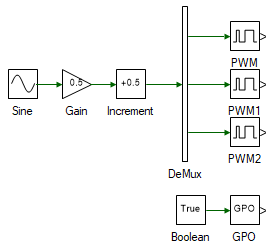
The real-time controller inside the three-inverter module has a dedictated PWM peripheral that can generate PWM pulses from duty cycle. It automatically generates the triangular carrier and compares the duty-cycles to generate the pulses. Hence the following tools that generated the triangle carrier and compared to reference to generate the switching pulses are no longer needed for real-time control. The tools which generate the reference signals are retained as shown below.

Separate the three duty cycles using a Demux tool.
The functionality of tools deleted in the previous step is replaced by the PWM Output tool from the Hardware Integration tool class. Add three of these and connect them as shown:
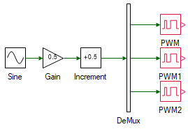
As can be seen in the above image, the three PWM blocks are highlighted in red which indicates an error. To view the cause of error, click the Messages tab in the bottom dock. This will bring the following window to view:

This error is thrown because the real-time controller that is being used is not mentioned. Not all controllers support PWM peripherals. To select a device, open project properties by double clicking on the project node in Explorer. In the Properties dock, click on the top-most drop-down menu which says: Simulation Settings, and select: Device Configuration. Within this, change the Device property from None to 3 Inverter. While at it, also change the following properties:
Frequency in PWM Configuration from 6000 to 10000
Waveform in PWM Configuration from Sawtooth to Triangle
Since the control algorithm no longer needs to generate the reference carrier, the model step time can be more relaxed. To increase it, open model properties, by double clicking anywhere on the model's blank space. Change the Step time to 0.001 in the Properties dock.
At this point, the initial error is replaced by new error. This error basically says that both the PWM peripherals point to the same channel. This will be cleared when the channels are set. For this experiment, Phase A and B of Inverter 1 will be used. In the properties of PWM1 tool, change the Channel from 1 to 2 and that of PWM2 tool's Channel from 1 to 3, which represents B and C phase gate signals respectively. Once this is set, both the errors disappear.
 Note
NoteAs long as there is any error, the model cannot be run.
By default, inverter outputs are held in high-impedance. To enable the inverter, to allow it to be actively driven, the reset pin must be pulled high. This is done by adding the following two blocks as shown and setting the properties given in table below:
| Tool name | Tool Class | Property field | Property value |
|---|---|---|---|
| Boolean | Signal Sources | Value | True |
| GPO | Hardware Integration | Channel | 1 |
Click the  icon in the top dock to save all the file.
 Warning
Ensure that the DC power supply is turned off. Avoid any accidental short-circuit in the following connections.
Connect the three-inverter module to the DC supply via the back panel. Connect the USB cable from the computer to the inverter module. Connect the DSO probe across the Phase A (black terminal) output of Inverter 1 and input DC bus negative (black terminal on the back panel of the inverter module). Similarly, connect another probe across Phase B (red terminal) output of Inverter 1 and input DC bus negative.
Click the  button on the top dock to transition from simulation to real-time mode.
 Warning
Take all necessary lab safety precautions.
Turn ON the DC power supply and set the voltage to 40 V. Click the  to run the system in real-time.
Observe the switching waveform on the DSO. Click  to halt the communication between the computer and the inverter.
This only stops the data transfer and not the inverter module, as can be seen with the switching pulses still being actively generated.
Change the output voltage in the Constant1 tool to a value between 0 and 40 and press the
  to run the inverter with the new duty.
Repeat this step for different output voltage reference values.
 Warning
Ensure that the probe attenuation is set to 10x to avoid over-loading the DSO.
Click  , Turn OFF the DC power supply.
Space vector PWM - Third harmonic injection:
Open the previously developed third-harmonic-injection simulation model.
Open project properties and change the Device property from None to 3 Inverter in the Device Configuration page. While at it, also change the following properties:
Frequency in PWM Configuration from 6000 to 10000
Waveform in PWM Configuration from Sawtooth to Triangle
Similar to real-time Sine-PWM implementation, remove all the tools other than those that generate the reference duty cycles. Add the PWM tools and GPO as before and set them to the same channel as done earlier. The final model after these modifications is shown below.
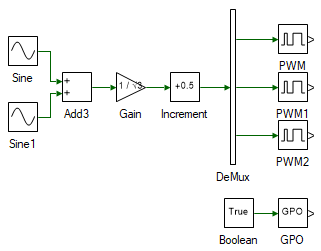
Change the model Step time to 0.001.
Click the  button on the top dock to transition from simulation to real-time mode.
 Warning
Take all necessary lab safety precautions.
Turn ON the DC power supply and set the voltage to 40 V. Click the  to run the system in real-time.
Observe the switching waveform on the DSO. Click  to halt the communication between the computer and the inverter.
This only stops the data transfer and not the inverter module, as can be seen with the switching pulses still being actively generated.
Change the output voltage in the Constant1 tool to a value between 0 and 40 and press the
  to run the inverter with the new duty.
Repeat this step for different output voltage reference values.
Click  , Turn OFF the DC power supply.
Space vector PWM - Min-max method:
Open the previously developed min-max simulation model.
Open project properties and change the Device property from None to 3 Inverter in the Device Configuration page. While at it, also change the following properties:
Frequency in PWM Configuration from 6000 to 10000
Waveform in PWM Configuration from Sawtooth to Triangle
Similar to real-time Sine-PWM implementation, remove all the tools other than those that generate the reference duty cycles. Add the PWM tools and GPO as before and set them to the same channel as done earlier. The final model after these modifications is shown below.
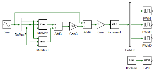
Change the model Step time to 0.001.
Click the  button on the top dock to transition from simulation to real-time mode.
 Warning
Take all necessary lab safety precautions.
Turn ON the DC power supply and set the voltage to 40 V. Click the  to run the system in real-time.
Observe the switching waveform on the DSO. Click  to halt the communication between the computer and the inverter.
This only stops the data transfer and not the inverter module, as can be seen with the switching pulses still being actively generated.
Change the output voltage in the Constant1 tool to a value between 0 and 40 and press the
  to run the inverter with the new duty.
Repeat this step for different output voltage reference values.
Click  , Turn OFF the DC power supply and disconnect all the connections including the USB.
This concludes the experiment of switched mode DC converter.
Attach separate screenshots of the simulation and real-time model for all three pwm control.
Attach screenshot of phase voltage Van and line-line voltage Vab for different modulation indices for all three pwm control.
Attach Phase A and Phase B voltage as observed on the DSO for different duty-cycles in real-time mode for all three pwm control.
Measure the output voltage, i.e. voltage at Phase A with respect to Phase B. This can be done by using the subtract function on the scope.
 Warning
Do not connect a (non-isolated) probe directly across Phase A and Phase B, especially when the USB is connected as this will lead to a ground loop with non-zero potential. Possibly destroying the computer, inverter module, and/or the DSO.
Verify if the frequency of the output voltage matches the set frequency. Check if the voltage matches the expected value. If not explain why.
For a DC bus voltage of 40V, what is the maximum balanced sinusoidal peak phase voltage attainable using the three pwm control schemes.