
In the previous experiment, Buck converter - Continuous conduction mode (CCM) was analyzed in continuous-conduction mode (CCM), i.e., the inductor current was always greater than 0. In this experiment, the buck converter operation under discontinuous-conduction mode (DCM) is analyzed. Unlike CCM, under DCM the inductor current briefly goes to 0 during each switching cycle.
A buck converter is shown below, with the transistor and the diode forming the two-position switch of the power pole.
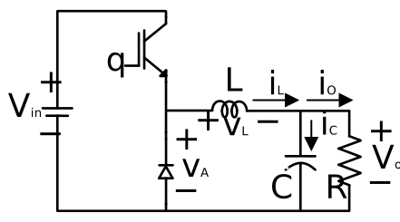
Similar to CCM operation, under DCM, turning on the transistor increases the inductor current, and when the transistor is turned off, the inductor current freewheels through the diode. During the freewheeling portion, as the energy stored in the inductor is dissipated in the load, the inductor current continues to fall until it reaches zero. If the next switching cycle begins before the current goes to zero, the converter is said to operate under CCM. Otherwise, if the current goes to zero and remains zero until the next switching cycle, the converter is said to operate under DCM. For a given transistor switching function waveform q(t), shown below, with a switch duty ratio d in steady state under DCM, the waveform of the voltage vA at the current port, for an ideal buck converter, is as shown below.
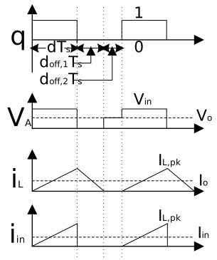
When the switch is ON, i.e., q(t) = 1, vA = Vin. When the switch is OFF but the inductor current iL is not yet zero, vA = 0. This is because the diode is conducting during this period. When the switch is OFF and the inductor current iL is zero, vA = Vo. This is because the diode no longer conducts and it blocks the full output voltage across it.
Since, under steady-state conditions, the average current through the output capacitor is zero and the average inductor current IL equals the output current Io
At the boundary of CCM and DCM, the average inductor current IL,crit equals half the peak inductor current
During the switch OFF time period (1 - d) × Ts, the inductor current drops from IL,pk to 0. During this period, the voltage across the inductor is Vo = d × Vin. Thus, the peak inductor current is
From Eqns. 1 through 3, solving for the load resistance value at which the buck converter is at the border of CCM and DCM
During CCM the relationship between the input and the output voltage is
This relationship is not valid under DCM. The new relationship can be derived by assuming that the converter is ideal and that there is no power loss within the converter. Therefore,
From the input current waveform above, the average input current is given by
From the inductor current waveform, the peak inductor current is given by
Substituting Eqn. 7 and Eqn. 8 into Eqn. 6
where \(M = \frac{R \times T_{s}}{2L} \times d^{2}\).
Solving the above quadratic equation yields
where
The above waveform was for an ideal buck converter. One stark difference between the ideal and actual response is the observed oscillation in vA and the inductor current iL during the doff,2Ts time period, as shown below.
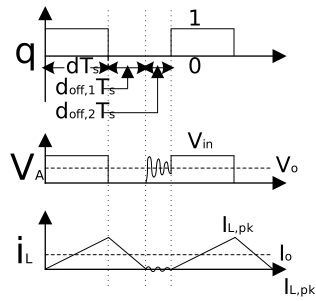
This is due to the fact that both the diode’s and the switch’s parasitic capacitances, along with the buck converter’s inductor, form an LC tank circuit, as shown below.
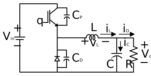
The tank circuit rings when the current is zero and the voltage across the diode changes rapidly, as is the case during the doff,2Ts time period. This ringing leads to increased electromagnetic interference (EMI) and higher losses. The frequency of this ringing is given by the natural frequency of the tank circuit
This model is exactly the same as the one used earlier in Buck converter - Continuous conduction mode (CCM).
Copy the folder containing the pre-built example project for this experiment, usually located at C:\Program Files (x86)\Sciamble\WorkBench v1\Examples\CUSPLab\BasicPowerElectronics\Experiment4, and paste it in a location where the user has permission to edit and save files, such as the Desktop folder.
Launch the Workbench application.
Open the pre-built example project that was pasted in Step 1.
Open the  Buck model within the project.
Ensure that the PWM switching frequency on the Device configuration page in the project properties is set to 100 kHz.
Ensure that the PWM channel is set to the Si power pole, i.e., Channel is set to 1.
This setup is exactly the same as the one used earlier in Buck converter - Continuous conduction mode (CCM).
 Warning
Before proceeding, ensure that the isolated power supply is powered down and that the USB cable is disconnected.
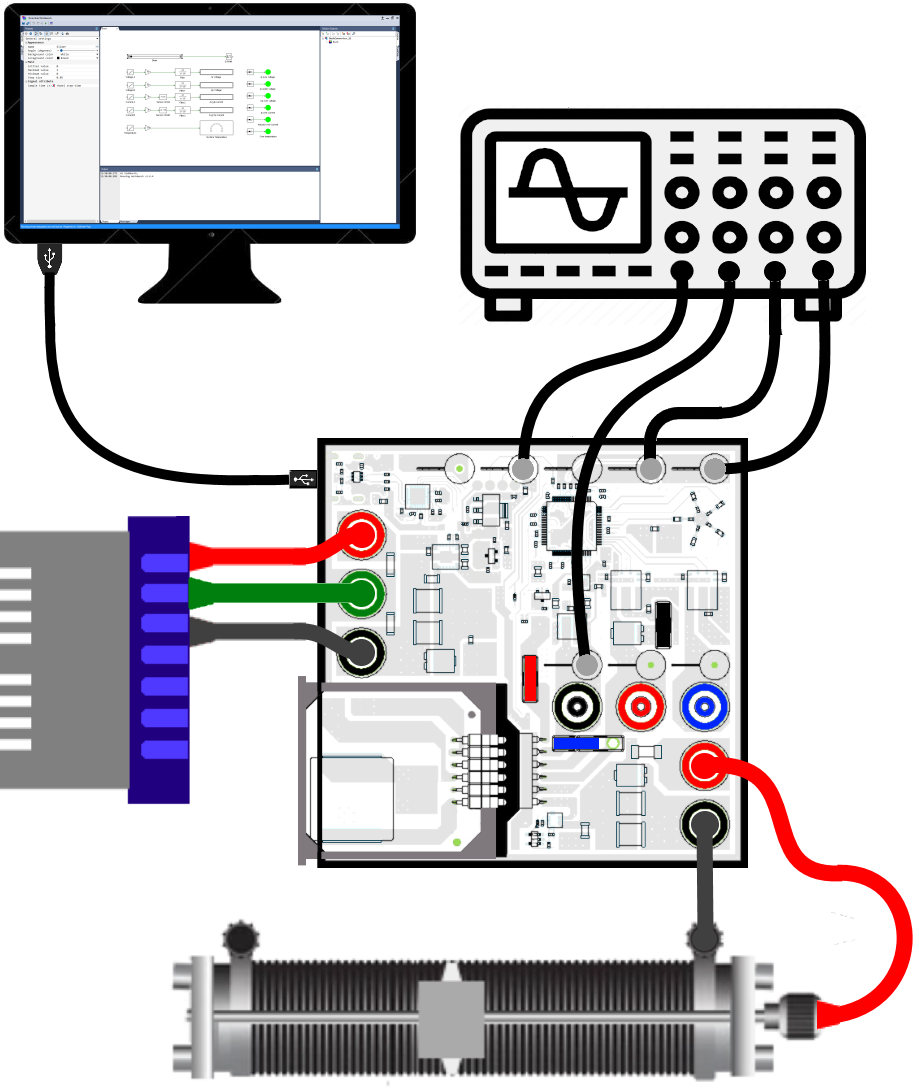
Magnetics card connection: Replace the existing magnetics card with the Buck/Boost/Buck-boost magnetics card, making sure that all six pins are properly aligned and in contact with the power-pole board, adjusting the angle if necessary.
WarningNever leave the magnetics card unscrewed. If contact is lost while the converter is running, interrupting the inductor current can produce a very high voltage, potentially damaging the converter or creating a safety hazard.
Rheostat setting: Set the slider such that the resistance across the two closest rheostat terminals is 10 Ω.
Power connections:
Connect the I+/I- terminals to the isolated power supply:
DC +ve: ● I+ (Red)
Ground: ● GND (Green)
DC −ve: ● I− (Black)Connect the O+/O- terminals to the rheostat load:
Rheostat rail: ● O+ (Red)
Rheostat terminal closest to the rail: ● O− (Black)DSO connections:
Connect DSO channel 1 probe to Ii. Set the following options, if they are supported by the DSO:
Set the probe to 1x.
Set the measurement type as Current.
Set the scaling factor to 4x.
Set the offset at 1.5 V or 6 A.
Set termination to 1 MHz.
Set the channel as inverted.
Connect DSO channel 2 probe to Io. Use the same settings as Channel 1.
Connect DSO channel 3 probe to Vo using the 20:1 attenuator. Set the following options, if they are supported by the DSO:
Set the probe to 1x.
Set the measurement type as Voltage.
Set the scaling factor to 20x.
Set the offset at 0 V.
Set termination to 1 MHz.
Set the channel as default/non-inverted.
Connect DSO channel 4 probe to Sa using the 20:1 attenuator. Use the same settings as Channel 3.
Jumper settings:
Insert jumpers ❶ and ❺ (●) to bypass the external current measurement.
Insert the GaN/Si jumper ❷ (●) to Sa/Sw. This connects the buck-converter inductor to the midpoint of the Si power pole.
Jumper ❸ (●) for the GaN FET’s external diode may remain inserted or removed, since this experiment does not use the GaN power pole.
Insert jumper ❹ (●) to connect the drains of the top switches to the positive DC bus (Vin+).
Remove jumper ❻ (●) to disconnect the capacitors across the switches.
Connect the USB cable to the power-pole board and the computer.
DC power supply settings:
Make sure that the DC power supply is fully turned down to 0 V prior to turning on the supply.
Turn on the power supply and gradually ramp up the voltage from 0 V to 15 V.
If the option is available, set the power supply current limit at 4.5 A.
The final wiring should look similar to this:
Click on the  icon in the top dock of Workbench to transition from the simulation mode to the real-time mode.
Click  to run the control algorithm in real time.
Gradually increment the duty cycle from 0 to 0.5.
Gradually increase the load resistance to the maximum possible value, using at least nine increments to make measurements: four in CCM, one at the boundary of CCM and DCM, and four in DCM.
At the boundary of CCM and DCM, the inductor current (DSO channel 2) goes to zero for just an instant.
Make the following measurements:
Make a note of the voltage and current values displayed on Workbench for each incremental change in the load resistance.
Observe the DSO waveforms and make a copy of the voltage across the diode (channel 4), the output voltage (channel 3), the inductor current (channel 2), and the input current (channel 1) for each incremental change in the load resistance. Adjust the time base to show between 4 and 10 switching cycles.
In DCM, make a note of the frequency of the ringing component in the measured voltage across the diode (channel 4).
Click on  to stop the model.
Repeat this section for a switching frequency of 40 kHz.
If required, repeat the same experiment using the GaN power pole instead of the Si power pole, as demonstrated in Switching characteristic of Si MOSFET/GaN FET and diode.
Attach the DSO waveforms showing the voltage across the diode, the output voltage, the inductor current, and the input current at a switching frequency of 100 kHz for varying load resistance.
Attach the DSO waveforms showing the voltage across the diode, the output voltage, the inductor current, and the input current at a switching frequency of 40 kHz for varying load resistance.
For a switching frequency of 100 kHz and a duty cycle of 0.5, enter the measured values from the Workbench screen capture and calculate the following values:
| Vin (V) | Vo (V) | Io (A) | R (Ω) | dcalc | dact |
|---|---|---|---|---|---|
where dcalc is 0.5 if in CCM and is given by Eqn. 10 if in DCM. \(d_{\mathrm{act}} = \frac{V_{o}}{V_{\mathrm{in}}}\) under both CCM and DCM. Load resistance \(R = \frac{V_{o}}{I_{o}}\).
Plot dcalc and dact as a function of the output current Io.
For a switching frequency of 100 kHz and a duty cycle of 0.5, compute Rcrit using Eqn. 4. Use the inductance value estimated in Buck converter - Continuous conduction mode (CCM) experiment. Compare this result with the measured value in the table above.
Repeat the same process for a switching frequency of 40 kHz and a duty cycle of 0.5.
Using Eqn. 11 and the measured ringing frequency under DCM, estimate the net parasitic capacitance, CD + CP.
"Power Electronics, A First Course," Ned Mohan and Siddharth Raju, Wiley Publication.

