


The objective of this experiment is to study an isolated full-bridge DC-DC converter under open-loop conditions (no feedback). The four switches apply alternating positive and negative voltage pulses to the transformer primary, while a center-tapped rectifier and LC filter produce a regulated-polarity DC output.
The full-bridge converter uses two switching legs. During one active interval, the upper switch of leg A and lower switch of leg B conduct, applying +Vin to the transformer primary. During the other active interval, the lower switch of leg A and upper switch of leg B conduct, applying -Vin. Between active intervals, the transformer primary voltage is zero and the output-inductor current freewheels through the rectifier.
Let d be the duration of each active diagonal-switch interval, normalized to the switching period Ts. Because there are two active intervals in every switching period, the rectified transformer-secondary voltage is present for a total duration of 2dTs. The duty cycle must remain below 0.5 so that a zero-voltage interval remains between the two bridge states.
Applying volt-second balance to the output inductor under continuous-conduction mode gives
The Full Bridge magnetics card is labeled with a 1:1:1 transformer ratio and a 68 µH output inductor. With Ns/Np = 1, the ideal relationship simplifies to Vo = 2dVin.
Copy the folder where the pre-built example project for this experiment is present, usually in C:\Program Files (x86)\Sciamble\WorkBench v1\Examples\CUSPLab\BasicPowerElectronics\Experiment14, and paste it in a location where the user has permission to edit and save files, such as the Desktop folder.
Launch the Workbench application.
Pin ( ) the Explorer dock on the right and the Toolbox dock on the left.
Click the second icon within the Explorer dock,  , to open the project.
Navigate to the folder where the example was pasted in Step 1. Double-click the FullBridgeConverter.project node to open the project.
Click the  icon to explore the project files.
Double-click the
icon to explore the project files.
Double-click the  FullBridge node to display the model.
Double-click the  FullBridgeConverter project node and open Device configuration.
Verify that Frequency is 100000 and Waveform is Triangle within PWM Configuration.
FullBridgeConverter project node and open Device configuration.
Verify that Frequency is 100000 and Waveform is Triangle within PWM Configuration.
Verify the four PWM tools in the model:
Ap PWM: Channel = 1, PWM Polarity = Normal.
Ap PWM1: Channel = 2, PWM Polarity = Flipped.
Bn PWM1: Channel = 3, PWM Polarity = Flipped.
Bn PWM: Channel = 4, PWM Polarity = Normal.
Open the Slider property and verify that its minimum, maximum, initial, and step values are 0, 0.45, 0, and 0.01, respectively. The Constant and Add tools generate the complementary 1-d command used by the flipped PWM channels.
 Warning
Before proceeding, ensure that the isolated power supply is powered down and that the USB cable is disconnected.
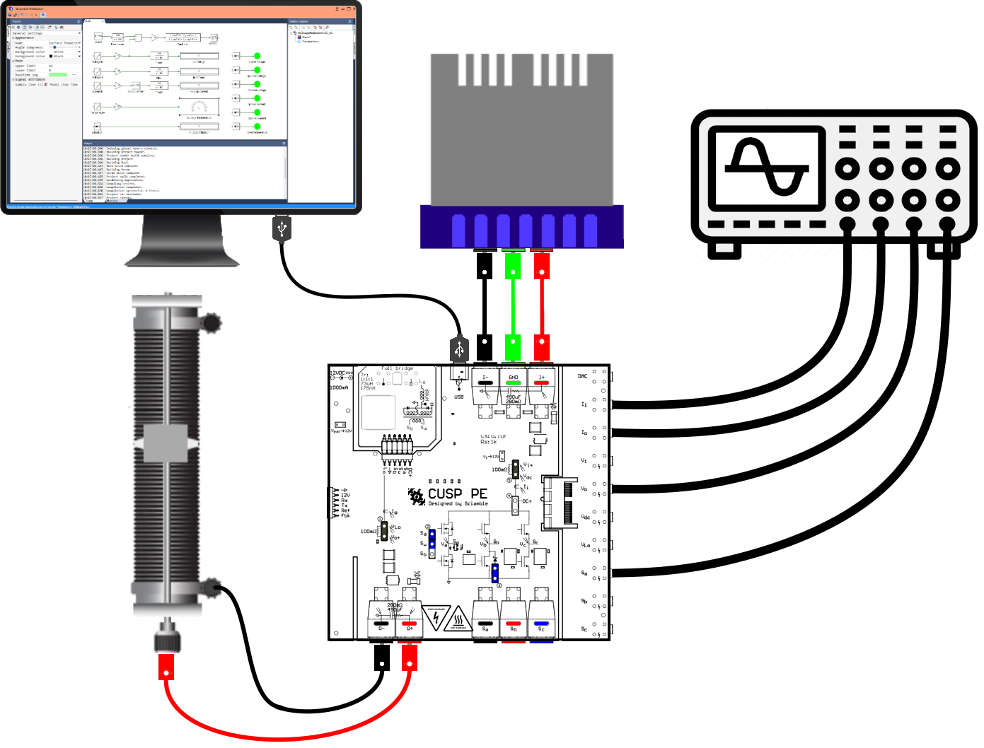
Magnetics card connection: Replace the existing magnetics card with the Full Bridge magnetics card, making sure that all six pins are properly aligned and in contact with the power-pole board, adjusting the angle if necessary.
WarningNever leave the magnetics card unscrewed. If contact is lost while the converter is running, the interruption of inductor current can create a very high voltage, potentially damaging the converter or creating a safety hazard.
Rheostat setting: Set the slider such that the resistance across the two closest rheostat terminals is 8 Ω.
Power connections:
Connect the I+/I- terminals to the isolated power supply:
DC +ve: ● I+ (Red)
DC −ve: ● I− (Black)Connect the O+/O- terminals to the rheostat load:
Rheostat rail: ● O+ (Red)
Rheostat terminal closest to the rail: ● O− (Black)Connect the power supply ground to the ground terminal on the board:
Ground: ● GND (Green)
DSO connections:
Connect DSO channel 1 probe to Ii. Set the following options, if they are supported by the DSO:
Set the probe to 1x.
Set the measurement type as Current.
Set the scaling factor to 4x.
Set the offset at 1.5 V or 6 A.
Set termination to 1 MHz.
Set the channel as inverted.
Connect DSO channel 2 probe to Io. Use the same settings as Channel 1.
Connect DSO channel 3 probe to Sa using the 20:1 attenuator. Set the following options, if they are supported by the DSO:
Set the probe to 1x.
Set the measurement type as Voltage.
Set the scaling factor to 20x.
Set the offset at 0 V.
Set termination to 1 MHz.
Set the channel as default/non-inverted.
Connect DSO channel 4 probe to Sb using the 20:1 attenuator. Use the same settings as Channel 3.
On the DSO, create the math trace Channel 3 - Channel 4 to display the transformer-primary voltage vpri = vSa - vSb.
WarningUse the board's attenuated S_a and S_b measurement terminals. Do not connect a grounded DSO probe directly across the two high-power switching terminals.
Jumper settings:
Insert jumpers ❶ and ❺ (●) to bypass the external current-measurement resistors.
Jumper ❷ (●) does not select either full-bridge leg; leave it between Sa and Sw for consistency with the preceding experiments.
Insert jumper ❸ (●) to connect the GaN leg's external freewheeling diode.
Insert jumper ❹ (●) to connect the high-side switch drains to the positive DC bus.
Connect the USB cable to the power-pole board and the computer.
DC power supply settings:
Make sure that the DC power supply is fully turned down to 0 V prior to turning on the supply.
Turn on the power supply and gradually ramp up the voltage from 0 V to 15 V.
If the option is available, set the power supply current limit at 4.5 A.
The final wiring should look similar to this:
WarningThe transformer provides functional isolation inside the full-bridge power stage, but the lab kit's measurement system references the input and output negatives to a common point. Treat the lab output as non-isolated.
Click on the  icon in the top dock of Workbench to transition from simulation mode to real-time mode.
Click  to run the control algorithm in real time.
If an undervoltage fault occurs, slightly increase the input voltage above 15 V but keep it below 16 V.
Stop the model by clicking  and rerun it.
Gradually increment the duty cycle from 0 to 0.4 in steps of 0.05. If a fault occurs, stop the model by clicking .
Make the following measurements:
For duty cycles of 0.1, 0.2, 0.3, and 0.4, capture the input current (channel 1), output-inductor current (channel 2), the two bridge midpoint voltages (channels 3 and 4), and the primary-voltage math trace (channel 3 - channel 4). Adjust the time base to show between 4 and 10 switching cycles.
For each duty-cycle step, record the values displayed by Ip Voltage, Op Voltage, Avg Ip Current, and Avg Op Current in Workbench.
WarningDo not exceed a duty cycle of 0.45. The zero-voltage interval is required to prevent overlap between the two diagonal bridge states.
Click to stop the model.
Turn OFF the power supply and disconnect the USB cable.
Attach the DSO waveforms showing both bridge midpoint voltages, the transformer-primary voltage, the input current, and the output-inductor current at 100 kHz for duty cycles of 0.1, 0.2, 0.3, and 0.4.
For duty cycles varying from 0.1 to 0.4 in steps of 0.05, enter the measured values from Workbench and calculate the following values:
| dset | Vin (V) | Iin,avg (A) | Pin (W) | Vo (V) | Io,avg (A) | Pout (W) | dact | Efficiency (%) |
|---|---|---|---|---|---|---|---|---|
For the card's 1:1 turns ratio, calculate the actual duty cycle using \(d_{\mathrm{act}} = \frac{V_{o}}{2V_{\mathrm{in}}}\).
Plot Vo and efficiency as functions of dset, and compare the measured voltage gain with Eqn. 1.
At a duty cycle of 0.4, measure the peak-to-peak output-current ripple and estimate the output inductance using \(L_{o} = \frac{(N_{s}V_{\mathrm{in}} - N_{p}V_{o}) \times d \times T_{s}}{N_{p} \times \Delta i_{L}}\). Compare the result with the 68 µH value printed on the Full Bridge magnetics card.
"Power Electronics, A First Course," Ned Mohan and Siddharth Raju, Wiley Publication.