Review Safety considerations when working in power electronics before proceeding.
There are three major components to the Workbench-based power electronics system, which will be used to perform all the experiments in this course. These are as follows:
Workbench simulation and rapid-prototyping software platform.
GaN/Si power module with on-board controller and data logger.
Magnetics and snubber card.
In this experiment, a pre-built buck converter open-loop control model is run in real time as an introduction to the components mentioned above. The following section gives a brief overview of the various components used to run the buck converter model. This will be followed by running the system in real time using the GaN/Si power electronics platform.
The overall system is shown in the figure below and consists of the following components:

Workbench software platform: A numerical simulation platform that supports both model- and code-based design. The toolbox within the platform consists of various pre-built arithmetic, logical, conditional, and storage operators that can be used to model complex systems by dragging and dropping these tools and interconnecting them. In addition to simulating a system, the platform can generate digital-controller-specific code that can be programmed into a microcontroller/digital signal processor to perform real-time control.
Isolated DC power supply: Used to power the converter DC bus as well as other auxiliary power stages for the gate driver, on-board controller, etc.
 Note
NoteThe communication channel between the computer and the three-inverter module is not isolated. Hence, the DC power supply must be isolated to avoid common-mode current, which could otherwise potentially damage the whole system.
USB COM channel: Code and data transfer happens via USB 2.0. Under ideal conditions, the maximum data transfer is 480 kbps, which translates to 15,000 samples per second of real-world variables such as average input and output currents, voltages, etc.
GaN/Si power-pole board: The hardware module contains all the power electronics, gate drivers, current and voltage sensors, digital signal processor, data logger, and programmer necessary for design, deployment, and real-time control of common DC-DC and DC-AC converters. There are two GaN power poles and one Si power pole, each rated 40 V, 5 A. Forced cooling using two frame-mounted fans allows the converter to be switched safely up to 250 kHz at rated conditions. Each power pole is independently controlled by the on-board TI TMS320F280049 digital signal processor (DSP).

In addition to PWM control of the power poles, the DSP reads feedback signals from current and voltage sensors on the DC bus, at the switching node, and the switch-heatsink junction temperature. The measured data, as well as other model variables, can be logged and viewed in real time in the Workbench software platform. This is enabled by a dedicated on-board data transfer link between the computer and the DSP. The same channel is also used to transfer the program from the computer to the DSP.
Plug-in magnetics card: Based on the converter under consideration, different magnetics cards are connected to the main board. There are 4 cards: Buck/Boost/Buck-boost, Flyback, Forward, and Full bridge. Depending on the jumper selection, the magnetics can connect to either the Si or the GaN power pole.

No magnetics card is needed for DC-AC experiments.
Rheostat load: A 50 Ω, 5 A, 100 W rheostat is used as the load for all the experiments.
Digital storage oscilloscope (DSO): The on-board data logger is limited in bandwidth and can thus only log average signals varying below ~100 Hz. To measure switching-frequency components, which are typically on the order of 100 kHz, a DSO is required. Review the MDO 3014 manual for instructions on how to use a DSO.
Non-isolated probes: The power-pole and magnetics boards have MCX connectors to measure various signals as listed in the table below. Use the MCX-to-BNC cable to connect these to the DSO.
The basic block diagram of the power-pole board is shown in the figure below
The simplified version of the actual board is shown in the figure below. The locations of the various components on the board are indicated in the following table.

Power terminals:
| Terminal designation | Location | Comments |
|---|---|---|
| I- | A6 | Negative DC bus terminal. |
| GND | A7 | Safety earth termination. Enclosure is tied to this terminal. |
| I+ | A8 | Positive DC bus terminal. |
| O- | J2 | Magnetics output/input negative terminal. |
| O+ | J3 | Magnetics output/input positive terminal. |
| SWA | J6 | Si power-pole midpoint. |
| SWB | J7 | GaN power-pole midpoint (with external free-wheeling diode). |
| SWC | J8 | GaN power-pole midpoint (without external free-wheeling diode). |
DSO measurement terminals:
| Terminal designation | Location | Scaling | Offset | Comments |
|---|---|---|---|---|
| DAC | A10 | 1 V ≘ 1 V | 0 V | Analog output synthesized by the controller. Used for observing digitally generated control signals. |
| Ii | B10 | 1 V ≘ 4 A | 1.5 V (or 6 A) | DC bus current. Current from the external power supply/load into the terminal is negative. |
| Io | C10 | 1 V ≘ 4 A | 1.5 V (or 6 A) | Magnetic circuit output current. Current from the terminal into the external power supply/load is negative. |
| Vi | D10 | 1 V ≘ 1 V | 0 V | DC bus voltage (before current sense resistor). |
| Vo | E10 | 1 V ≘ 1 V | 0 V | Magnetic circuit output voltage (after current sense resistor). |
| Vdc | F10 | 1 V ≘ 1 V | 0 V | DC bus voltage (after current sense resistor). |
| VLo | G10 | 1 V ≘ 1 V | 0 V | Magnetic circuit output voltage (before current sense resistor). |
| SWA | H10 | 1 V ≘ 1 V | 0 V | Si power-pole midpoint voltage. |
| SWB | I10 | 1 V ≘ 1 V | 0 V | GaN power-pole midpoint voltage (with external free-wheeling diode). |
| SWC | J10 | 1 V ≘ 1 V | 0 V | GaN power-pole midpoint voltage (without external free-wheeling diode). |
| ⬤ | A2 | 1 V ≘ 1 V | 0 V | Buck inductor output, flyback secondary, forward secondary, and full-bridge inductor voltage. The measurement point is indicated by 📍 (test-point symbol) on the magnetics card. |
| ■ | A3 | 1 V ≘ 1 V | 0 V | Buck switch node, flyback snubber capacitor, forward tertiary, and full-bridge secondary voltage. The measurement point is indicated by 📍 (test-point symbol) on the magnetics card. |
 Warning
It is recommended to use the 20:1 attenuator while measuring voltage at terminals marked with ↯ symbol. DSO analog channels typically tolerate a maximum of 5 V rms with peaks up to ±20 V.
Jumpers:
The jumpers are organized by color based on their functionality:Black (●): when present, these jumpers bypass the sense resistor for high-precision external current measurement.
Blue (●): when present, these jumpers modify the response of the circuit and are not critical for proper operation.
Red (●): critical jumpers that modify the circuit connection—improper use can potentially damage the circuit.
| Jumper designation | Color | Location | Comments |
|---|---|---|---|
| ❶ | Black (●) | F2 | When disconnected, the magnetic-circuit output current can be measured by measuring the voltage difference between the VLo and Vo measurement terminals. When connected, the sense resistor is bypassed. This jumper is typically connected. |
| ❷ | Blue (●) | G4 | When the jumper is inserted between the terminals marked Sa and Sw, the output of the Si leg is connected to the magnetic circuit. Alternatively, when the jumper is inserted between the terminals marked Sb and Sw, the output of the GaN leg is connected to the magnetic circuit. |
| ❸ | Blue (●) | H6 | When the jumper is connected, the external antiparallel free-wheeling diode is connected in parallel across the bottom switch of the SWB GaN power pole. Otherwise, the reverse current freewheels through the GaN device, leading to significant losses. This jumper is typically connected. |
| ❹ | Red (●) | E7 | When the jumper is connected, the high-side (top) switches of the power pole are connected to the positive DC bus (I+). Otherwise, these switches’ drain terminals are left floating—needed for topologies that rely only on the low-side (bottom) switches. |
| ❺ | Black (●) | D7 | When disconnected, the DC bus current can be measured by measuring the voltage difference between the Vi and Vdc measurement terminals. When connected, the sense resistor is bypassed. This jumper is typically connected. |
| ❻ | Red (●) | B4 (Buck-converter) | When the jumper is connected, 4.7 nF capacitors are connected across the switches for soft-switching. This jumper is typically disconnected, except for the soft-switching experiment. |
| ❻ | Red (●) | B4 (Flyback-converter) | When the jumper is connected, the snubber circuit is connected to the primary side. |
| ❻ | Blue (●) | B4 (Forward-converter) | When the jumper is connected, the snubber circuit is connected to the primary side. |
 Note
NoteThe presence or absence of jumpers ❶ and ❷ does not affect the internal current measurement displayed in Workbench, nor does it affect the current at the measurement terminals. Both are handled through a separate sense amplifier. The external current measurement provides an alternative, high-precision option without amplifier-induced delays or slew effects.
Shunts:
There are two shunts/jumpers at C1 and D7 that select the power source for the gate drivers and cooling fans. At any time, exactly one must be connected.
Other connections:
| Location | Comments |
|---|---|
| A5 (bottom) | USB-C port for programming and data logging. Ensure the cable side marked with a white dot is facing up. |
| E1 (bottom) | Active MOSFET-based load control terminals. Not needed if the load is a rheostat. Active load allows for remote control of the load. |
Indicators:
| Location | Comments |
|---|---|
| E3 (bottom) | Buzzer. Emits a rising-frequency beep when the input voltage exceeds 24 V. If an over-current, over-voltage, over-temperature, or DC bus under-voltage fault occurs, the buzzer beeps five times. After this, the controller must be reprogrammed from Workbench to clear the fault. |
| E5 | Green LED. Blinking indicates insufficient input voltage (below 14 V). Solid green indicates sufficient input voltage (14 V–22 V) or input above the safe limit (less than 24 V). |
| E5 | Red LED. ON indicates output terminal over-voltage (default threshold: above 24 V). |
| E5 | Red LED. ON indicates DC bus under- or over-voltage (default thresholds: below 14 V or above 24 V). |
| E4 | Red LED. ON indicates DC bus over-current (default threshold: above 4 A). |
| E4 | Red LED. ON indicates magnetics card output terminal over-current (default threshold: above 4 A). |
| E4/E5 | All red LEDs ON indicates heatsink–device junction over-temperature (default threshold: above 85 °C). |
Copy the folder containing the pre-built example project for this experiment, usually in C:\Program Files (x86)\Sciamble\WorkBench v1\Examples\CUSPLab\BasicPowerElectronics\Experiment1, and paste it in a location where the user has permission to edit and save files, like the Desktop folder.
Click the  icon on the desktop to launch the application.
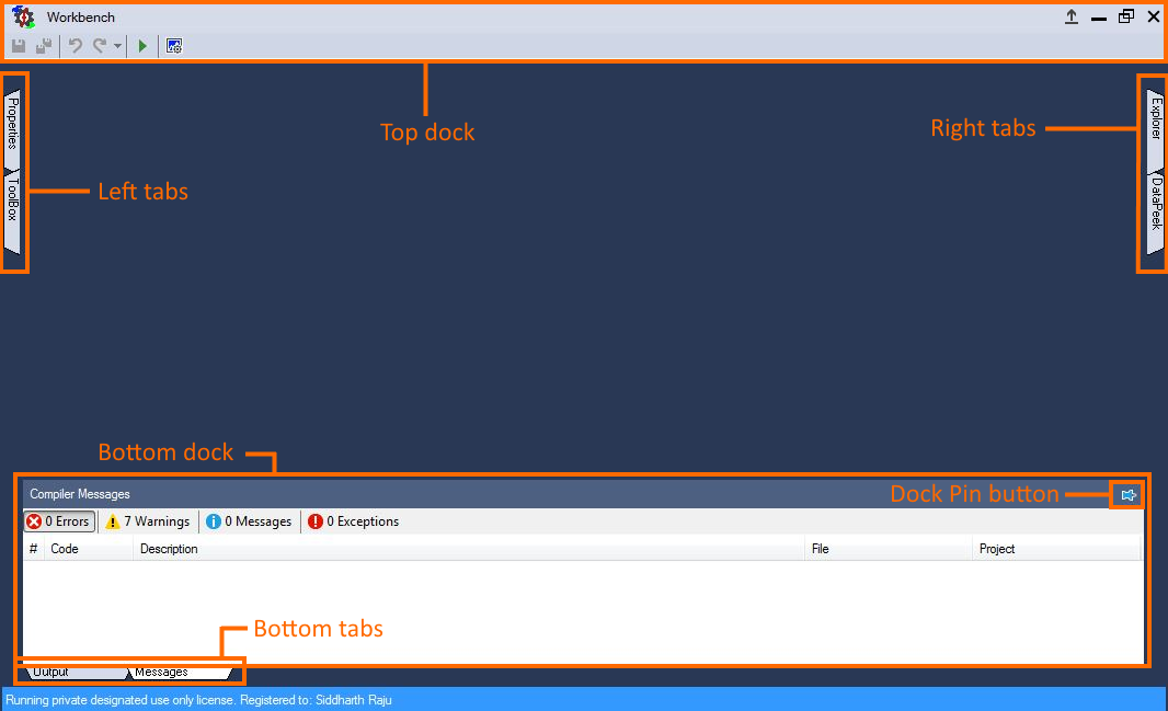
Workbench has tabs on the left, right, and bottom that represent docked windows, each conveying or controlling different pieces of information.

Clicking these tabs reveals their respective docked windows. The content within these docks changes based on context, as will be seen later.
Click the Toolbox tab on the left tabs section and pin the window by clicking the  icon on the top-right corner. Similarly, pin the Explorer dock on the right.
The tools in the Toolbox are grouped into categories based on their operation. Click the drop-down list
  to navigate between tool classes.
Click the  icon in the Toolbox dock to hide the toolbox for now.
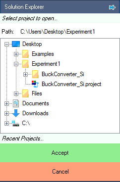
The Explorer/Solution Explorer dock acts as both a file browser to navigate to and open, add, or remove files from the project, as well as a container to display the project structure.
The toolbar within the Explorer dock  consists of the following buttons:
 : Creates a new project.
 : Opens an existing project.
 : Creates a new model or script file and adds it to the selected project.
 : Adds an existing model or script file to the selected project.
 : Removes the selected project, model, or script file. This does not delete it from the physical folder; it simply removes it from the current project.
 : Permanently deletes (sends to Recycle Bin) the selected model or script file.
 : Download project files.
Click the second icon,  , to open an example project. This opens the file browser within the Explorer dock.
Navigate to the folder where the pre-built example project was pasted in Step 1. Double-click the BuckConverter_Si.project node within that folder to open the project.

Click the  icon to explore the files within the project.
To display the model file, double-click the
  Buck node in the Explorer dock.

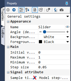
Double-click the slider block labeled Slider to open its properties in the Property dock on the left.

In real time, as the slider is incremented, the converter duty cycle varies from 0 to 1 in steps of 0.05.
 Warning
Before proceeding, ensure that the isolated power supply is powered down and that the USB cable is disconnected.
Magnetics card connection: Detach the backplate by unscrewing the four screws, two on each side, and slide out the existing magnetics card. Insert the Buck/Boost/Buck-boost magnetics card, making sure that all six pins are properly aligned and in contact with the power-pole board, adjusting the angle if necessary. Once the card is in place, reattach the backplate and secure it firmly with the screws.
 Warning
Never leave the magnetics card unscrewed. If contact is lost while the converter is running, it has the potential to cause very high voltage due to interruption of inductor current, potentially damaging the converter, or worse, could lead to a safety hazard.
Rheostat setting: Set the slider such that the resistance across the two closest rheostat terminals is 10 Ω.
Power connections:
Connect the I+/I- terminals to the isolated power supply:
DC +ve: ● I+ (Red)
Ground: ● GND (Green)
DC −ve: ● I− (Black)Connect the O+/O- terminals to the rheostat load:
Rheostat rail: ● O+ (Red)
Rheostat terminal closest to the rail: ● O− (Black)DSO connections:
Connect DSO channel 1 probe to Ii. Set the following options, if they are supported by the DSO:
Set the probe to 1x.
Set the measurement type as Current.
Set the scaling factor to 4x.
Set the offset at 1.5 V or 6 A.
Set termination to 1 MHz.
Set the channel as inverted.
Connect DSO channel 2 probe to Io. Use the same settings as Channel 1.
Connect DSO channel 3 probe to Vo using the 20:1 attenuator. Set the following options, if they are supported by the DSO:
Set the probe to 1x.
Set the measurement type as Voltage.
Set the scaling factor to 20x.
Set the offset at 0 V.
Set termination to 1 MHz.
Set the channel as default/non-inverted.
Connect DSO channel 4 probe to Sa using the 20:1 attenuator. Use the same settings as Channel 3.
Jumper settings:
Insert jumpers ❶ and ❺ (●) to bypass the external current measurement.
Insert the GaN/Si jumper ❷ (●) to Sa/Sw. This connects the buck-converter inductor to the midpoint of the Si power pole.
Jumper ❸ (●) for the GaN FET’s external diode may remain inserted or removed, since this experiment does not use the GaN power pole.
Insert jumper ❹ (●) to connect the drains of the top switches to the positive DC bus (Vin+).
Remove jumper ❻ (●) to disconnect the capacitors across the switches.
Connect the USB cable to the power-pole board and the computer. Ensure the side of the cable marked with a white dot is facing up when plugged into the board.
DC power supply settings:
Make sure that the DC power supply is fully turned down to 0 V prior to turning on the supply.
Turn on the power supply and gradually ramp up the voltage from 0 V to 15 V.
If the option is available, set the power supply current limit at 4.5 A.
The final wiring should look similar to this:

Click the  icon in the top dock of Workbench to transition from simulation mode to real-time mode,
where the control algorithm is executed in real time on the DSP. The generated gate signals, based on the duty cycle, are relayed to the gate drivers.
The measured average feedback signals are read by the ADC and relayed back to Workbench, where they are displayed on the Scopes.
 Note
NoteWhen in real-time mode the top dock changes color from light blue to light salmon. In this mode, pressing Run will immediately download the program to the connected real-time controller and begin execution. Any previously programmed code will be lost. All necessary laboratory safety precautions must be taken.
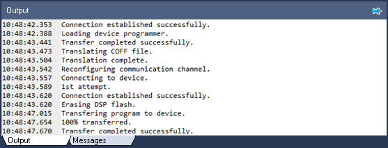
Click  to run the control algorithm in real time. The following message will be displayed if code has been transferred successfully:

If programming fails, check the USB connection and try again.
Once programmed, increase the duty cycle by clicking the slider “+” button. Increase gradually since sudden increases could lead to high transient current that could trigger an over-current fault.
If that occurs, stop the model by clicking the  button and re-run the model.
Vary the duty cycle from 0 to 0.9 and observe the switching-cycle waveforms on the DSO:

Also observe the average values displayed in Workbench.
Click  to stop the model.
Turn OFF the power supply and disconnect the USB cable.
This concludes the experiment. This experiment was a cursory introduction to various concepts that will be revisited in subsequent experiments.
Attach screenshots of the Workbench model display for different duty cycles.
Attach DSO waveforms for different duty cycles.
Go through further resource material on various features of Workbench available here.