


In the previous experiment, a prebuilt DC motor speed-control model was simulated and executed in real time. In this experiment, one of its components, the switched-mode converter, will be explored in further detail. The next section covers the theoretical background for this experiment, followed by the simulation of a switched-mode DC converter. Finally, the simulation model is verified in real time.
Consider the half-bridge converter shown below:
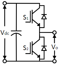
At no instant can both switches be simultaneously ON because this would cause shoot-through by directly shorting the DC bus. When switch S1 is ON, the output voltage is Vo = Vdc. When switch S2 is ON, the output voltage is Vo = 0. If S1 is switched ON for a duration Ton and S2 is switched ON for a duration Toff alternately, then the average output voltage is given by Eqn. 1. In pulse-width modulation, the sum Ton + Toff is held constant and is called the switching period, Tprd. Its inverse gives the switching frequency. As Ton is varied from 0 to Tprd, the output voltage varies between 0 and Vdc. The duty cycle is the fraction of the switching period for which switch S1 must be held ON to generate the desired output voltage, as given in Eqn. 2.
The half-bridge converter allows the generation of only a unipolar output voltage of variable magnitude. This limitation is overcome by using the full-bridge converter shown below:
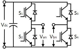
The output voltage is given in Eqn. 3, where Van and Vbn are the output voltages of the two half-bridges with respect to the DC bus negative. The duty cycle for each half-bridge is given in Eqns. 4 and 5.
This configuration allows the output voltage to be varied between +Vdc and -Vdc. When Vo is positive, dutyA > 0.5 and dutyB < 0.5; when it is negative, dutyA < 0.5 and dutyB > 0.5. dutyA is the ratio of the ON time of switch S1 to the total switching period. dutyB is the ratio of the ON time of switch S3 to the total switching period.
To generate the gate signal for switch S1 from dutyA, the duty cycle is compared with a triangular carrier that varies from 0 to 1. The triangular carrier repeats every 1/fswitch, where fswitch is the desired switching frequency.
The above operation is simulated in this section using Workbench.
Open Workbench and create a new model file as follows:
Click  to open the application.
Pin ( ) the Explorer dock on the right and the Toolbox dock on the left.
Within the toolbar in the Explorer dock, click the  /1st icon to create a new project file.
Give it a suitable name and location, and click Accept to create a new project. This adds a .project file and a folder with the same name as the project
to house the project files.
/1st icon to create a new project file.
Give it a suitable name and location, and click Accept to create a new project. This adds a .project file and a folder with the same name as the project
to house the project files.
A project can contain multiple model and code files. This experiment requires only a single model file. To add this file, first select the newly created
project node in the Explorer dock. To add a file to the selected project, click the  /3rd icon in the Explorer
toolbar. The following window will open:
/3rd icon in the Explorer
toolbar. The following window will open:
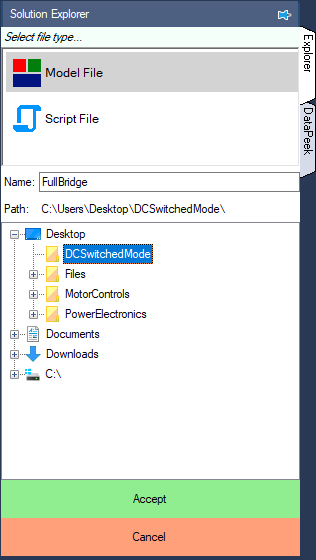
Change the file name from UntitledFile to FullBridge. The path by default will point to the newly created project folder. Leave it as it is. Click Accept to add the new model file to the project.
 Note
NoteThe project must be selected for the New File icon to become active.
Drag and drop the following tools from the Toolbox onto the open model.
Triangle - Signal Sources.
Mag-Time Scope - Display.
The Triangle tool is present within the Signal Sources tool class and Scope is present in the Display tool class. Use the drop-down menu in the Toolbox to transition between the tool classes.
Connect the output of the Triangle tool to the input of Scope.
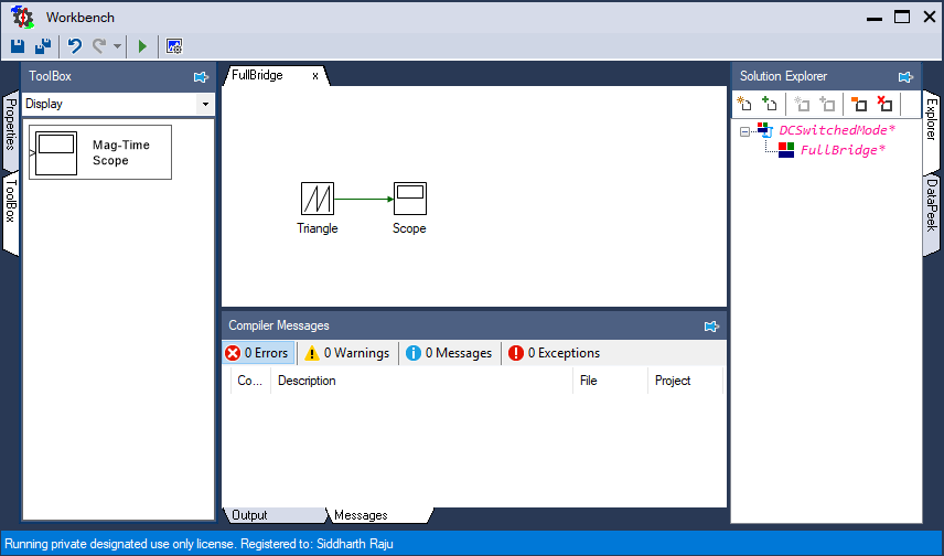
Click  in the top dock to run the simulation. This will produce the following error in the Output window in the bottom dock.
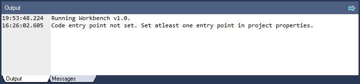
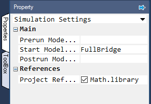
As mentioned earlier, a project can contain multiple files, so the compiler must be told which file is the starting point. In this case, there is only one file, and it should be set as the starting point. To do this, double-click the project node in the Explorer. This should display the project properties in the Properties dock on the left. Within the properties, set the Start model/Function field to the name of the model file, i.e., FullBridge, as shown below:
Once again, click the in the top dock to run the simulation. The simulation should run successfully this time as can be inferred from the messages in the Output dock.
Double-click the Scope block in the model to view the simulation result. The following window will pop up:
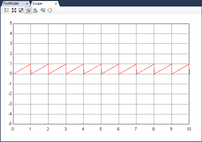
Double-click anywhere on the plot, or click the  /3rd icon on the scope's toolbar, to automatically focus the result.
A 1 Hz switching frequency is too low for typical motor-control applications. A switching frequency of 10 kHz is used for all the experiments. Also, a triangular carrier is preferred over a sawtooth carrier because it reduces lower-order switching-frequency harmonics. To make these changes, go back to the model file and double-click the Triangle tool to reveal its properties in the Properties dock. Change the Frequency (Hz) from 1 to 10000.
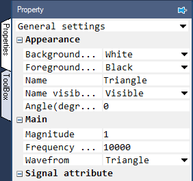
Also change the Waveform from Sawtooth to Triangle. Rerun the simulation.
Open the scope to view the results. Automatically focusing the result shows only random spikes close to zero. This is because the simulation is being "refreshed" at a much slower rate than needed to process and capture sufficient data points. To fix this, the simulation step time should be one hundredth of the triangular carrier's period, Tprd, which equals 1/(10 kHz)/100 = 1E-6 s. To do this, double-click anywhere in the blank space in the model file. This opens the model properties in the Properties dock. Change the Step time from 0.01 to 1E-6. While at it, change the Run time from 10 to 1E-3.
Rerun the simulation and observe the scope result. Verify that the frequency, waveform, and magnitude are as expected. So far, the carrier waveform has been generated. In the next few steps, this carrier will be compared with the reference voltage to generate the switching signals.
Drag and drop tools 3 through 12 listed in the table below, from the Toolbox, in addition to the tools 1 and 2 already added, as shown:
| # | Tool type | Tool class | Tool name |
|---|---|---|---|
| 1 | Triangle | Signal Sources | Triangle |
| 2 | Mag-Time Scope | Display | Scope |
| 3 | Constant | Signal Sources | Constant |
| 4 | Constant | Signal Sources | Constant1 |
| 5 | Gain | Math Block | Gain |
| 6 | Adder Subtractor | Math Block | Add |
| 7 | Adder Subtractor | Math Block | Add1 |
| 8 | Comparison operator | Logical Block | Comparator |
| 9 | Comparison operator | Logical Block | Comparator1 |
| 10 | Boolean-Numeric cast | Signal Conversion | Type cast |
| 11 | Boolean-Numeric cast | Signal Conversion | Type cast1 |
| 12 | Mag-Time Scope | Display | Scope1 |
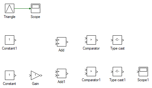
Click the link connecting Triangle and Scope, and delete it. Reposition the Scope and interconnect the tools as shown.
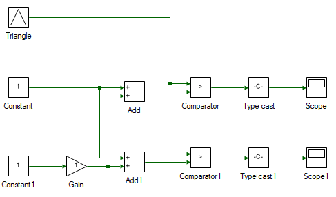
Change the properties of each tool to the values listed in the table below. The reasons for these values are given in the rightmost column. To access a tool's properties, double-click the tool; its properties will appear in the Properties dock.
| Tool name | Property field | Property value | Comments |
|---|---|---|---|
| Triangle | Frequency | 10000 | Carrier/switching frequency is 10 kHz. |
| Triangle | Waveform | Triangle | - |
| Constant | Magnitude | 0.5 | Center point in Eqns. 4 and 5. |
| Constant1 | Magnitude | 5 | This is the desired output voltage. |
| Gain | Gain | 1/(2*40) | 1/(2*Vdc) in Eqns. 4 and 5. Vdc = 40 V. |
| Add | No change | Output of this block is dutyA in Eqn. 4. | |
| Add1 | Arithmetic operation | +- | Output of this block is dutyB in Eqn. 5. |
| Comparator | Function | < | Compares the triangle carrier to dutyA and, if the former is less, outputs True; otherwise, it outputs False. |
| Comparator1 | Function | < | Compares the triangle carrier to dutyB and, if the former is less, outputs True; otherwise, it outputs False. |
| TypeCast | No change | True/False does not have an intrinsic numeric value. This tool converts True to 1 and False to 0. Other values can also be chosen in the properties. |
Rerun the simulation and observe the results in the scopes. Scope shows the gating signal for switch S1, and Scope1 shows the gating signal for switch S3. The gating signals for switches S2 and S4 are, in theory, complementary to the gating signals for switches S1 and S3, respectively.
Change the output voltage from 5 to the following values: 0, 40, 20, and 10. Observe the dutyA and dutyB waveforms.
The simulation above is run in real time in this section.
The real-time controller inside the three-inverter module has a dedicated PWM peripheral that can generate PWM pulses from the duty cycle. It automatically generates the triangular carrier and compares the duty cycles to generate the pulses. Hence, the following tools are no longer needed and must be deleted from the model: Triangle, Comparator, Comparator1, TypeCast, TypeCast1, Scope, and Scope1.
The functionality of the tools deleted in the previous step is replaced by the PWM Output tool from the Hardware Peripheral tool class. Add two of these tools and connect them as shown:
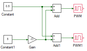
As shown in the image above, the two PWM blocks are highlighted in red, indicating an error. To view the cause of the error, click the Messages tab in the bottom dock. This will display the following window:
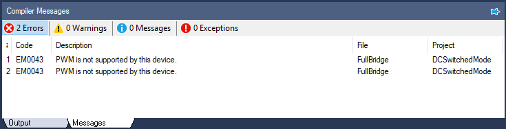
This error occurs because the real-time controller being used has not been specified. Not all controllers support PWM peripherals. To select a device, open the project properties by double-clicking the project node in Explorer. In the Properties dock, click the topmost drop-down menu, which displays Simulation Settings, and select Device Configuration. Within it, change the Device property from None to 3 Inverter. Also change the following properties:
Frequency in PWM Configuration from 6000 to 10000
Waveform in PWM Configuration from Sawtooth to Triangle
Since the control algorithm no longer needs to generate the reference carrier, the model step time can be increased. To increase it, open the model properties by double-clicking anywhere in the model's blank space. Change the Step time to 0.001 in the Properties dock.
At this point, the initial error is replaced by a new error. This error indicates that both PWM peripherals point to the same channel. It will be cleared when the channels are set. For this experiment, phases A and B of Inverter 1 will be used. In the properties of the PWM1 tool, change the Channel from 1 to 2, which represents the phase-B gate signal. Once this is set, both errors disappear.
NoteIf there are any errors, the model cannot be run.
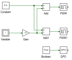
Replace the Constant1 tool with a Variable tool from the Runtime Source tool class in the Toolbox.
By default, the inverter outputs are held at high impedance. To enable the inverter so that it can be actively driven, the reset pin must be pulled high. This is done by adding the following two blocks, as shown, and setting the properties given in the table below:
| Tool name | Tool Class | Property field | Property value |
|---|---|---|---|
| True/False | Signal Sources | Value | True |
| Digital Output | Hardware Integration | Channel | 1 |
Click the  icon in the top dock to save all the files.
 Warning
Ensure that the DC power supply is turned off. Avoid any accidental short-circuit in the following connections.
Connect the three-inverter module to the DC supply via the back panel. Connect the USB cable from the computer to the inverter module. Connect the DSO probe across the phase-A output (black terminal) of Inverter 1 and the input DC bus negative (black terminal on the back panel of the inverter module). Similarly, connect another probe across the phase-B output (red terminal) of Inverter 1 and the input DC bus negative.
Click the  button in the top dock to transition from simulation to real-time mode.
WarningTake all necessary lab safety precautions.
Turn ON the DC power supply and set the voltage to 40 V. Click to run the system in real time.
Observe the switching waveform on the DSO. Change the output voltage in the Variable tool to a value between 0 and 40 to change the inverter duty cycle. To edit the value of the Variable tool in real time, click the tool to display the on-screen numpad shown below:
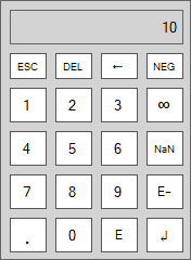
Click DEL to clear the existing value, enter the new value, and press ENTER ↲. You can also type the value using the keyboard instead of the on-screen numpad. Repeat this step for different output-voltage reference values.
WarningEnsure that the probe attenuation is set to 10x to avoid overloading the DSO.
Click  , turn OFF the DC power supply, and disconnect all connections, including the USB cable.
This concludes the experiment on the switched-mode DC converter.
Attach separate screenshots of the simulation and real-time model.
Attach screenshots of the results in Scope and Scope1 from the simulation model for the different reference voltages specified.
Attach the phase-A and phase-B voltages observed on the DSO for different duty cycles in real-time mode.
Measure the output voltage, i.e., the voltage at phase A with respect to phase B. This can be done using the subtract function on the scope.
WarningDo not connect a (non-isolated) probe directly across Phase A and Phase B, especially when the USB is connected, since this will lead to a ground loop with non-zero potential, and possibly destroying the computer, inverter module, and/or the DSO.
Verify that the frequency of the output voltage matches the set frequency. Check whether the voltage matches the expected value. If not, explain why.